Disclosure: when you buy through links on our site, we may earn an affiliate commission.

CMOS Analog Circuit Design – Amplifiers with Solved Examples

Learn to design successfully CMOS Amplifier, Current Mirrors and Active Loads
3.7
3.7/5
(10 reviews)
95 students
Created by

8.4

CourseMarks Score®

10.0

Freshness

7.0

Feedback

7.6

Content

Platform: Udemy
Video: 6h 15m
Language: English
Next start: On Demand

Table of contents

Description

“Analog circuit design is like chess – just because you know how the pieces move doesn’t mean you know how to play the game”. – Patrick Lahey

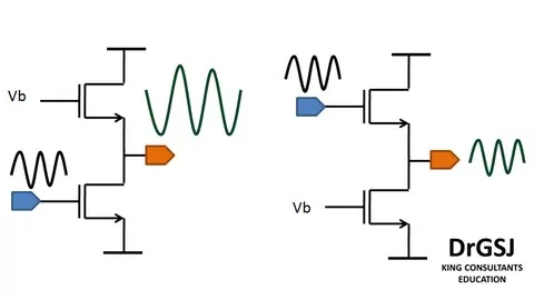
This course is a continuation of another Analog IC Design “CMOS Analog IC Design – MOSFET, DC BIAS and Transconductance”. This 6 hour course allows you to learn, design and analyze CMOS amplifiers, Current Mirrors and Active loads in detail. Each topic has multiple (atleast 4) worked out examples to allow hands on design.
Consequently, we’re seeing analog job requisitions in several key areas including Sensor Design and Sensor interfaces, WiFi (wireless LANs and Internet access), ultra wide band technology (UWB) and power management. Demand for designers with expertise in high-speed data conversion seems to be high across a variety of industries.
We would like to thank Dr Mohammed Hashimi, IIITD for agreeing to use his lecture slides to educate the Analog Circuit Design Community across the world.

You will learn

✓ Understanding the details of MOSFET characteristics
✓ Transconductance Gm
✓ Understand the requirements for an analog IC designer
✓ Small Signal Analysis of Circuits
✓ Calculate the small signal Gain, Input and output impedance and signal swing

Requirements

• Students should have an interest in the topic of analog IC design.
• Attend the “CMOS Analog IC Design – MOSFET, DC BIAS and Transconductance” course on Udemy
• Knowledge of DC Biasing and maintaining the devices in saturation

This course is for

• Curious students about the devices and potential nano-engineering students
• Aspiring Analog IC designers who need to brush up their knowledge on CMOS Amplifiers
• Undergraduate students who are beginning to learn Analog IC Design
• Post Graduate Students who need a refresher course
Design Thinker and Analog IC Design Manager
Dr G S Javed obtained his M.S. and Ph.D. from the Indian Institute of Science, Bangalore in 2016 for his work on low power integrated instrumentation circuits for sensing applications. From 2016 to 2020, he led and managed a 15 member transceiver design team in Terminus Circuits. He worked on high-speed wireline transceivers (upto 20 Gbps) focusing on the Receiver design, high speed RO and LC PLLs (upto 16 GHz), and CT Sigma Delta ADCs. From August 2008 to July 2010, he worked as Deputy Engineer with Integrated Circuit Design Center(ICDC), Bharat Electronics Limited (BEL).He enjoys photography, travel and meeting people.
He serves as a reviewer for many IEEE Transactions, Journals and Conferences. He is an invited speaker for specialized technical areas like Clocking Solutions, High Speed Links and Capacitance Sensor Interfaces and non-technical areas like Design Thinking and Problem Solving, Research Methodologies, Technical Writing and Entrepreneurship Skills.
Browse all courses by on Coursemarks.
Platform: Udemy
Video: 6h 15m
Language: English
Next start: On Demand

Students are also interested in